Google Ironwood TPU: From Bits to HBM
💡 Foundation AI Seminar Series

This week’s Foundation seminar for the AI by Hand Academy focused on TPUs. I walked through the system from the most basic 0/1 bits all the way up to high-bandwidth memory (HBM), building the full picture step by step in a beginner-friendly, by-hand ✍️ way.
I was also fortunate to be joined by a special guest expert, Shanya Chaubey from Micron Technology, who helped answer participants’ HBM questions live in the chat and added valuable industry perspective throughout the session.
Below is an early sketch of the memory hierarchy drawing I used during the seminar.
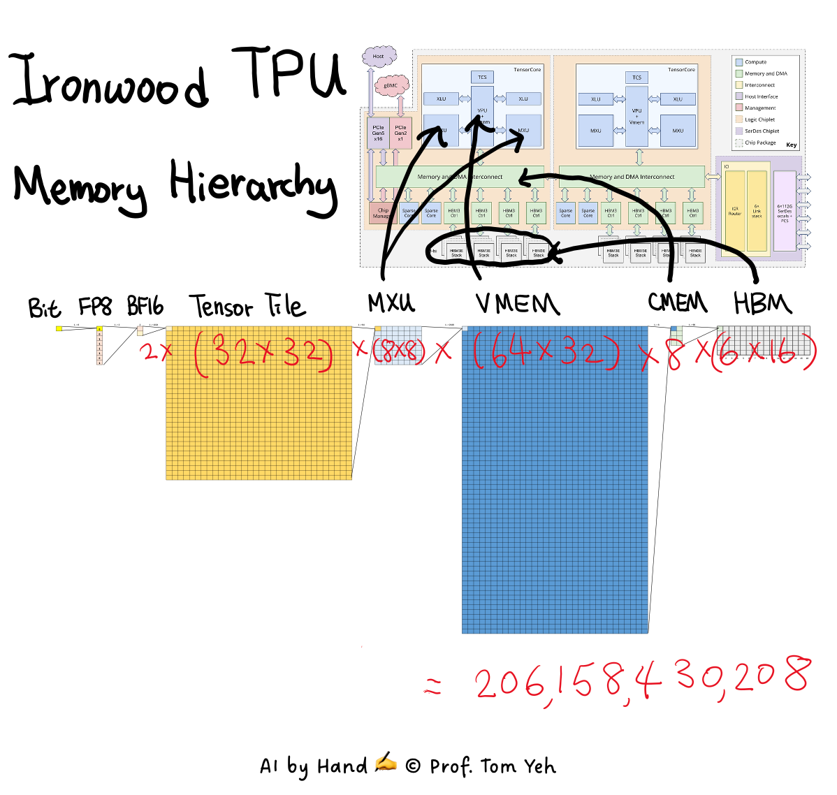
Bit – The most basic unit of information, the on–off decision from which every number, tensor, and model state is ultimately constructed.
FP8 (1×8 → 8 bits) – Eight bits are grouped to form a floating-point value, typically used for inference, where reduced precision is a deliberate trade-off to maximize throughput and efficiency.
BF16 (×2 → 16 bits) – Two FP8-scale chunks are combined to gain more dynamic range and stability, while still staying friendly to high-throughput hardware.
Tensor tile (×1024 → 1K) – Data moves through the chip in blocks of 1024 values at a time, defining the granularity at which tensors are fetched and manipulated.
Matrix Multiplication Unit (MXU) (×64 → 64K) – A systolic array where matrix multiplication is not abstract but physical, with tensor tiles flowing through fixed hardware to achieve the highest possible throughput.
Vector Memory (VMEM) (×2048 → 128M) – On-chip working memory that holds activations, partial results, and intermediates, sized specifically to keep the systolic array busy without stalling.
Shared Memory (SMEM) (×8 → 1 GB) – A small but critical shared memory sitting between VMEM and HBM, used for staging, accumulation, synchronization, and cross-lane coordination.
HBM (×96 → 96 GB) – Off-chip high-bandwidth memory where model weights and large states live, implemented as HBM3e with 16 stacks at 6 GB each, for a total of 96 GB.
Dual-Die (×2 → 192 GB) – Two tightly coupled compute dies operate as a single logical accelerator, each with its own local HBM, effectively doubling memory capacity and bandwidth while allowing tensors and activations to stream seamlessly across dies as if they lived on one chip.
Outline
Google Ironwood TPU
Memory Hierarchy
High Bandwidth Memory (HBM)
Shared Memory (SMEM)
Vector Memory (VMEM)
Matrix Multiplication Unit (MXU)
Recording & Excel Workbook